Review PCB layout ZIGBEE/ADC

Thread Starter

waulu

Joined Dec 23, 2016
62
Hello,

I have designed a small PCB to use at home. It will be some kind of device for a smart home, the goal is to control the heater automatically through the relays, control the lighting through ZIGBEE and detect if there's someone in bed with a load sensor. This will be a shield to connect to the Attiny817 Xplained Mini. I have attached the schematic of the circuit that I designed. The board will be power supplied by the USB Micro connector. I will solder the components by hand.

schematic.png

I would like someone to indicate improvements over the layout.

1) I am worried about the U1 ADS1231, I couldn't find a layout recommendation. This IC is analog so I don't know if the placement is correct.

2) What do you think about the placement of the capacitors around the U1 and U2?

3) The connector J5 belongs to the ZIGBEE module, 410-201, because it's analog too, should I create a separate ground for it?

4) I still have layer 3 free, I don't know what is the best thing to do with that one.

5) What about the ramification of the 5V on the bottom layer? The traces have 40 mils, it should be more than enough.

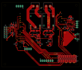
TOP Layer 1 :

TOP_layer1.png

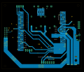
BOTTOM Layer 4 :

BOTTOM_layer4.png

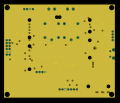
GND Layer 2 :

GND_layer2.png

Thank you in advance.
 
Last edited:
jpanhalt

Joined Jan 18, 2008
11,087
Here are a few suggestions:
1597146143262.png
Change the pinout to J7, if permissible:

1597146298509.png

You seem to have vias that do nothing, like on the trace J4-5 and J4-6
 

Thread Starter

waulu

Joined Dec 23, 2016
62
Thank you jpanhalt.

I changed the layout according to your recommendations. I have one question :

6) Why changing the pinout of J7 is important?

About the vias on J4-5 and J4-6, I am using them but it's hard to understand through the one layer image. I will add an image with TOP and BOTTOM layer superimposed.

The new layout is :

TOP (1) and BOTTOM (4) layer:

TOP_BOTTOM_Layer1_4.png

TOP (1) Layer :

TOP_Layer1.png

Bottom (4) layer :

BOTTOM_Layer4.png

GND (2) layer :

GND_Layer2.png
 

jpanhalt

Joined Jan 18, 2008
11,087
Thank you jpanhalt.

I changed the layout according to your recommendations. I have one question :

6) Why changing the pinout of J7 is important?

About the vias on J4-5 and J4-6, I am using them but it's hard to understand through the one layer image. I will add an image with TOP and BOTTOM layer superimposed.

The new layout is :
Re: #6
That was a question for you. I had no way to know whether the pinout for J7 was defined by what it connected to. If it's not important then you can change. One thing I consider with pinhead connectors is what will happen of the mating connector is attached wrong (reversed).

For example, say you have pins: signal1, VCC,GND, signal2. Reversing that will reverse the power, which is usually not good to do. Using a 5 pin connector for examle: singal1,GND,VCC,signal2,blank will avoid that problem. Of course, there can be many variations on that theme, but keep in mind what happens if the connector is reversed. Now, if you use shrouded or keyed connectors, that consideration is less significant.

There are probably other details that one could modify, not so much errors and slight improvements. Is schematic and board are consistent and pass DRC (design rules check), major errors, like shorts, are probably not present. Then you can start looking for more subtle things, like is the layout around an IC consistent with what the manufacturer recommends? Are decoupling capacitor in the best positions? Are signal lines appropriated isolated to avoid cross-talk? Are ground and power traces large enough to minimize heat (i.e., current capacity) and inductance? Stitching of ground planes? Potential ground loops?

Here's a well-know tutorial that is now a bit old, but the principles haven't changed: http://alternatezone.com/electronics/files/PCBDesignTutorialRevA.pdf

Regards/
 

Thread Starter

waulu

Joined Dec 23, 2016
62
That was a question for you. I had no way to know whether the pinout for J7 was defined by what it connected to. If it's not important then you can change. One thing I consider with pinhead connectors is what will happen of the mating connector is attached wrong (reversed).
Yes, I understand that, in this case the order of the pinout is not important. I will be connecting long wires to that connector. Yes, that's a good point, "what will happen of the mating connector is attached wrong (reversed)". I didn't think about how to minimize that, I will consider it.


Change the pinout to J7, if permissible:

1597146298509.png
But here you show some preference for a different way of routing the IC to the connector. And it's not related to safety measures I think so, right? My question is why do you prefer this way?

There are probably other details that one could modify, not so much errors and slight improvements. Is schematic and board are consistent and pass DRC (design rules check), major errors, like shorts, are probably not present. Then you can start looking for more subtle things, like is the layout around an IC consistent with what the manufacturer recommends? Are decoupling capacitor in the best positions? Are signal lines appropriated isolated to avoid cross-talk? Are ground and power traces large enough to minimize heat (i.e., current capacity) and inductance? Stitching of ground planes? Potential ground loops?
Thank you for the guidelines. I couldn't find the layout recommendations for the ADS1231. I have to take a look at the cross-talk, I didn't consider it, should I consider it for the signals SPI and I2C? What is the purpose of stitching the ground plane? I didn't consider ground loops too. I will take a look at these things.

Here's a well-know tutorial that is now a bit old, but the principles haven't changed: http://alternatezone.com/electronics/files/PCBDesignTutorialRevA.pdf
I will read it today or tomorrow.

Thank you again jpanhalt.
 

jpanhalt

Joined Jan 18, 2008
11,087
But here you show some preference for a different way of routing the IC to the connector. And it's not related to safety measures I think so, right? My question is why do you prefer this way?
It seemed a little shorter. I don't like going around things, and it had better clearance around the nearby capacitor. If that cap is decoupling, it can now be moved closer. Albeit, that suggestion was mostly personal preference. The other suggestions were better founded.

I enjoy routing, and make an arbitrary decision when to stop. Except for very simple designs, there is probably no single correct solution.
 

Thread Starter

waulu

Joined Dec 23, 2016
62
It seemed a little shorter. I don't like going around things, and it had better clearance around the nearby capacitor. If that cap is decoupling, it can now be moved closer. Albeit, that suggestion was mostly personal preference. The other suggestions were better founded.

I enjoy routing, and make an arbitrary decision when to stop. Except for very simple designs, there is probably no single correct solution.
Yes, you are right, now I can move the capacitor closer to the IC.

Thank you
 

Thread Starter

waulu

Joined Dec 23, 2016
62
Hello,

I still didn't read the whole document, but there's a part that mentions that boards that work with mains 220VAC should take that into consideration. I searched a little a bit and according to IPC-2221, I should have a big clearance and creepage between those traces to avoid flashover. To avoid ground under it is a good move too.

So, remove ground was easy but respect the clearances and creepages is much harder now, my question is :

7) The traces are short, it's just between the pins of the relays, do I really have to take into consideration the IPC-2221?

If the safety of the equipment or myself is in risk, of course, I will redo the layout.

EDIT : Maybe I could just delete the traces and solder a wire between the pins, for example, a 10 AWG.

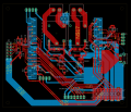
I updated the layout :

TOP and BOTTOM (1 and 4) Layer :

TOP_BOTTOM_Layer1_4.png

TOP (1) Layer :

TOP_Layer1.png

BOTTOM (4) Layer :

BOTTOM_Layer4.png

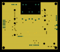
GND (2) Layer :

GND_Layer2.png
 
Last edited:
Top