diode in a b amplifier

Thread Starter

ntetlow

Joined Jul 12, 2019
63
i've just joined this forum having been learning electronics as a hobby for some months. i've been looking at amplifiers class AB in https://www.electronics-tutorials.ws/amplifier/class-ab-amplifier.html. I have two questions if someone will answer me:-
1) Why is the diode biasing at Vin plus or minus 0.7volts when the two resistors R1 and R2 and Vcc have an effect too?
2) I thought the diodes would block negative current from Vin from reaching the transistors, they seem to be treated purely as resistance?

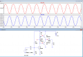
Mod: Added a AB amp image.E
amp1.PNG
 
Last edited by a moderator:

MrAl

Joined Jun 17, 2014
11,480
Hi,

Those diodes are used for proper drive of the two transistors.
The two transistor base emitter voltages are approximately equaled by the two diodes, so the base can "follow" the input signal yet be at a different voltage level. So the diodes are used for the proper voltage drop or voltage increase relative to the input voltage.
Note the voltage at the two emitters is approximately equal to the input voltage at the junction of the two diodes. The two transistors only provide for a current gain for the load.
Also note that the circuit after that one requires two diode voltage drops so two are used in series.
 

Thread Starter

ntetlow

Joined Jul 12, 2019
63
Thank you for your reply. The input sine wave has a positive and negative part? My point is how can the positive part get through to be amplified by the transistor TR1 whan the diodes are facing the wrong way and will block positive current.
 

ericgibbs

Joined Jan 29, 2010
18,849
hi nt,
Consider if the junction of the two diodes is at 12V/2 , when there is no input signal, this means there must be a current flowing from the 12V to 0V via the two resistors and the diodes.
The incoming signal +/- will change the current thru the diodes etc, and at the junction of the two diodes the voltage will rise and fall, switching on the appropiate output transistor.
E
 

MrAl

Joined Jun 17, 2014
11,480
Hello,

I think the mod entered the wrong schematic in post #1 so here is the right one:

When the input signal is zero the diode D1 prevents R1 from driving TR1. When the input signal goes high D1 conducts less thus allowing R1 to power the transistor base. TR1 thus conducts more to drive the load higher. When the input goes negative the same thing happens except with R2, D2, and TR2. R2 drives the base of TR2.
So the diodes do not drive the bases. The respective resistors drive the bases.

Amplifier-1.gif
 

Thread Starter

ntetlow

Joined Jul 12, 2019
63
Looking at the lspice neither va or vb has any negative voltage. Does this mean that only TR1 is being turned on? Am I wrong in thinking that a PNP transistor has a negative bias?
 

ericgibbs

Joined Jan 29, 2010
18,849
hi,
You have to consider the Base voltages of the transistors 'relative' to the transistors Emitter., not with respect to 0v.
E
 

Thread Starter

ntetlow

Joined Jul 12, 2019
63
I am getting disillusioned here. The explanations given in tutorials do not make a comprehensive explanation of what is really going on. Are they oversimplifying things. I know that different tutorials are seem to go into different levels of explanation. Is there any chance there is something out there that tells me just what is going on!
 

ericgibbs

Joined Jan 29, 2010
18,849
h nte,
OK, lets take a step back.
Do you know how a transistor works and also the difference between a NPN and a PNP type.?
I would like to try to help you with this problem.
E

BTW: I have updated post #6 image to show the Vbe voltages.
 

MrAl

Joined Jun 17, 2014
11,480
I am getting disillusioned here. The explanations given in tutorials do not make a comprehensive explanation of what is really going on. Are they oversimplifying things. I know that different tutorials are seem to go into different levels of explanation. Is there any chance there is something out there that tells me just what is going on!
Hello again,

Replace each diode with a voltage source of 0.7v with the polarity as if it was always forward biased.
Then see if you can figure out how it works.

When a diode is always forward biased it looks like a small voltage source like a battery except for the fact that it always absorbs energy rather than deliver it, but this is a side issue.
 

BobTPH

Joined Jun 5, 2013
8,961
Take the diodes out and see what the behavior would be with a signal of 2V peak to peak. If you can figure that out, then the effect of adding in the diodes will be easier to understand.

Bob
 

iimagine

Joined Dec 20, 2010
511
Looking at the lspice neither va or vb has any negative voltage. Does this mean that only TR1 is being turned on? Am I wrong in thinking that a PNP transistor has a negative bias?
To understand this circuit, you have to first learn how a CE (Common Emitter) transistor amplifier works, how to bias a transistor.
 

MrChips

Joined Oct 2, 2009
30,806
Another way to look at it, remove the GND symbol at the lower power rail and replace 0V supply with -Vcc.
Now you have a symmetrical circuit operating between +Vcc and -Vcc.
 

ericgibbs

Joined Jan 29, 2010
18,849
hi agu,
Many thanks for the heads up!.
I am still struggling to get Win10 & LTS XVII up and running., paying more attention to the bugs I keep encountering, than the circuit,,, damn.

Eric
 
Try this:

Without the diodes, you get class B operation. Only one transistor would be turned on at a time. There would also be crossover distortion because the input signal has to exceed +0.7 or -0.7 (the Vbe drops) before the corresponding transistor conducts.

The diodes make it class AB if your lucky. Part tolerances with no signal will make one of the output transistors to conduct more.
Those diodes should be thermally mounted to the transistors. As Vbe changes with temperature, the diode drop changes too.
 
Top