Hello!
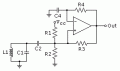
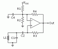
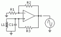
This circuit is an LC oscillator with a digital output, using single supply ( 5V GND )OP-AMP.
I have been trying to understand this circuit step by step, but two days, nothing. Can anyone explain the operation of this circuit step by step like; "... at initial position this has this voltage and after this charges this happens so opamp is in this mode and the output is this so it makes ..." . Thanks everyone!
The circuit schematic is added. And also I want to add the Falstad Circuit Simulator codes for you to import:
Rich (BB code):
$ 3 5.0E-6 32.755850052045055 54 5.0 50
a 376 248 456 248 1 5.0 0.0 1000000.0
r 376 328 456 328 0 47000.0
w 376 264 376 328 0
w 456 328 456 248 0
g 280 328 280 376 0
l 152 232 152 328 0 1.0 -0.00261395817586732
c 248 232 248 328 0 9.999999999999999E-6 0.6658661804968603
w 248 328 152 328 0
w 152 232 248 232 0
O 456 248 504 248 1
w 360 168 360 232 0
w 360 232 376 232 0
c 280 328 376 328 0 1.0E-5 -2.4853614377662505
w 248 328 280 328 0
c 360 232 248 232 0 9.999999999999999E-6 2.5009190426051853
R 248 88 232 88 0 0 40.0 5.0 0.0 0.0 0.5
r 248 88 360 168 0 100000.0
r 360 232 280 328 0 100000.0
w 456 168 456 248 0
r 456 168 360 168 0 100000.0
O 504 376 520 376 0
o 9 64 0 42 9.353610478917778 9.765625E-55 0 -1
o 6 64 0 34 1.25 0.003125 1 -1
Last edited: