Why don't books show you this?

Thread Starter

Eduard Munteanu

Joined Sep 1, 2007
86
Hi,

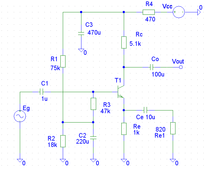
Take a look at the attached schematic. Most (all?) books will start by telling you to connect V1 (input) in parallel to R2 through a capacitor.

However, this is problematic, because you end up with crippled input impedance unless you bootstrap. Even bootstrapping isn't perfect, since it introduces positive feedback with its own problems. You also absolutely need an input capacitor.

Let's take a look at my schematic again. My arrangement is in fact equivalent to creating a split supply from a single supply, except for the poor ground impedance (high), located midway between R1 and R2. So in fact we treat the circuit as having 3 power rails: +Vcc/2, 0V, -Vcc/2.

The advantages are:
  1. No input coupling capacitor is needed if we know there's no DC on the line.
  2. Input impedance isn't sacrificed. If Q1 was a MOSFET, we would benefit from the full gate impedance.
  3. Coupling stages is easier, since we can make the ground reference stiffer and use it throughout the circuit, in an easy fashion.
  4. Bootstrapping isn't required, unless very very high impedances are needed.

In fact, there's another advantage to this. The ground reference can be made as stiff as we want without reducing input impedance and without consuming large amounts of power, perhaps using an op-amp.

A lot of literature out there insists on single-supply-ish biasing, even though creating a split supply is easy. My question is: why? Am I missing something?

EDIT: Yes, I know I forgot the 0V connection, sorry :). Consider R2 lower end connected to Vcc's supply ground.
 

Attachments

Wendy

Joined Mar 24, 2008
23,429
Actually, there is a major flaw in your schematic. The bias scheme is part of the transistor circuit, and the AC is introduced from outside the schematic, requiring you to define a common point (AKA, ground) between the transistor and the source. I can think of no example where your schematic applies.

This subject has been well discussed here at AAC, and will be again, since it is basic to understanding transistor amplifiers.
 

Thread Starter

Eduard Munteanu

Joined Sep 1, 2007
86
Actually, there is a major flaw in your schematic. The bias scheme is part of the transistor circuit, and the AC is introduced from outside the schematic, requiring you to define a common point (AKA, ground) between the transistor and the source. I can think of no example where your schematic applies.
Yes, my fault, I didn't specify the ground point. It's between R1 and R2. As I said, this is equivalent to putting the ground point between two equal supplies. But aside from this, it works.

And R2's lower end is connected to Vcc's zero volts wire. I apologise for the confusion, should've used a battery instead of Vcc.

As for split supply common-emitter BJT amplifiers, they need no explicit base biasing.
 

Thread Starter

Eduard Munteanu

Joined Sep 1, 2007
86
I attached another schematic which will hopefully eliminate all confusion. Please take a look at it.

In the rightmost schematic, Vcc and Vee are only rails, not sources.
 

Attachments

t_n_k

Joined Mar 6, 2009
5,455
Hi Eduard,

How would you apply this approach to a common emitter design (say with Av=20) - rather than the common collector case you have shown?

Also suppose you want to have several stages of amplification in tandem - how would you arrange the biasing / signal earthing?

Rgds,

t_n_k
 

steveb

Joined Jul 3, 2008
2,436
I attached another schematic which will hopefully eliminate all confusion. Please take a look at it.

In the rightmost schematic, Vcc and Vee are only rails, not sources.
Actually, I'm still confused. Is the output taken relative to the ground, or relative to the other end of the emitter resistor?
 

studiot

Joined Nov 9, 2007
4,998
I think communication would be better served if you stuck with conventional layout and labelling. They were, after all developed for good reasons.

For instance why does your signal input (AC) have + and - signs?

Unless everthing is floating you need to indicate what is physically connected to
earth. If you are floating everything then your arrangement will be very subject to hum and noise pickup.

We are all happy here to help you consolidate your ideas, so keep trying.
 

Thread Starter

Eduard Munteanu

Joined Sep 1, 2007
86
For instance why does your signal input (AC) have + and - signs?
That is a SPICE sine voltage source. If you connect it as I did, you get a normal sine wave, if you connect it in reverse (+ to ground, - to base) you get a negated sine wave, i.e. \(v(t) = - sin(\omega t) = sin(\omega t + \pi)\).

So basically, plus is the signal pin, while minus is the input's ground pin.

Unless everthing is floating you need to indicate what is physically connected to
earth. If you are floating everything then your arrangement will be very subject to hum and noise pickup.
Consider the input signal source a separate device, that is floating with respect to this amplifier unless the amplifier's ground is connected to the source as I did.

I don't float anything besides that, in fact I don't float anything more than in an ordinary, single supply amplifier driven by an external source.

We are all happy here to help you consolidate your ideas, so keep trying.
Thanks, I hope this clears things a bit.
 

Thread Starter

Eduard Munteanu

Joined Sep 1, 2007
86
t_n_k said:
How would you apply this approach to a common emitter design (say with Av=20) - rather than the common collector case you have shown?

Also suppose you want to have several stages of amplification in tandem - how would you arrange the biasing / signal earthing?
Actually, I'm still confused. Is the output taken relative to the ground, or relative to the other end of the emitter resistor?
It doesn't actually matter, since there's only a DC offset (exactly 4.5V) between ground and either power supply terminal. Let's say we pick ground as a reference point, which is a natural choice.

Chaining multiple stages should be done just like chaining split supply op-amps: DC coupling. This actually requires a common-emitter stage, because in my schematic the output will be a \(V_{BE}\) drop below ground (so you'd need a coupling capacitor).
 
Last edited:

t_n_k

Joined Mar 6, 2009
5,455
Hi Eduard,

You didn't answer my question about biasing a common emitter stage with the input source connected to a reference ground and directly driving the bjt's base - as in your common collector implementation. Or is it only possible to use this approach in the common collector case? Perhaps you could provide a circuit diagram to illustrate if you believe it can be done. I'm of course thinking of a stable (against variation in Beta and temperature) biasing outcome as one can achieve with the conventional resistor divider on the base side and emitter resistor for DC bias stability feedback.

Rgds,

t_n_k
 

Jony130

Joined Feb 17, 2009
5,488
Why don't books show you this
Simply, the book show principles only. Its up to designer to improve the circuit.

And equivalent AC-circuit look like this


So we are forced to add a capacitor and resistor which will provide path for DC base current after disconnecting input source.
And finally we end-up whit this classic circuit:


And opamp example
[/quote]

Besides, nowadays nobody besides amateurs use this simple circuit.
In real life situation we always can add a BJT to further improvements.

 
Last edited:

Ron H

Joined Apr 14, 2005
7,063
Eduard, what types of real world voltage sources do you think would work in this configuration? Dynamic microphones come to mind. Other than that...:confused:
 
Top