Problems with back to back MOSFET dimmer for 24VAC

Thread Starter

Lars Englund

Joined Dec 31, 2016
17
I've been trying, unsuccessfully, to dim a incandescent light bulb with two back to back mosfets similar as in this post: http://easy-electronics4u.blogspot.se/2012/02/switch-ac-loads-using-mosfets-as-relay.html but with transformer isolated 24VAC.

My circuit looks like this:

http://pasteboard.co/gXA6q1dRx.png
The lamp has been replaced with a 1K resistor in my tests.

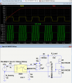
Below is the output from my scope:

http://pasteboard.co/gXBOr8Ok2.png
Scope ground clip is connected to 24VAC_B.
C1: 24VAC_A, C2: + (pin 3) of Diode_Bridge, C3: Drain of Q12, C4: DIM_GPIO

The load only gets every other half wave. Thinking about the circuit I feel that it will be impossible to get a Vgs voltage that is higher than the voltage at the source pin since the source pin will see the peak of the 24VAC? Is there a way (preferably simple & cheap :)) of solving this kind of double mosfet dimmer?

(Note to moderators: I previously posted a similar post about high voltage but I have changed my source to a safe isolated 24VAC, I'm only interested in learning more about electronics and MOSFETs here)
 
Last edited:

AlbertHall

Joined Jun 4, 2014
12,346
Your circuit won't work unless the power for the light is isolated from the power used for the gate drive, which is not the case in your circuit.
 

ronv

Joined Nov 12, 2008
3,770
I've been trying, unsuccessfully, to dim a incandescent light bulb with two back to back mosfets similar as in this post: http://easy-electronics4u.blogspot.se/2012/02/switch-ac-loads-using-mosfets-as-relay.html but with transformer isolated 24VAC.

My circuit looks like this:

http://pasteboard.co/gXA6q1dRx.png
The lamp has been replaced with a 1K resistor in my tests.

Below is the output from my scope:

http://pasteboard.co/gXBOr8Ok2.png
Scope ground clip is connected to 24VAC_B.
C1: 24VAC_A, C2: + (pin 3) of Diode_Bridge, C3: Drain of Q12, C4: DIM_GPIO

The load only gets every other half wave. Thinking about the circuit I feel that it will be impossible to get a Vgs voltage that is higher than the voltage at the source pin since the source pin will see the peak of the 24VAC? Is there a way (preferably simple & cheap :)) of solving this kind of double mosfet dimmer?

(Note to moderators: I previously posted a similar post about high voltage but I have changed my source to a safe isolated 24VAC, I'm only interested in learning more about electronics and MOSFETs here)
Take a look at this one. Don't forget the transformer!
 

Attachments

crutschow

Joined Mar 14, 2008
34,407
Here's an LTspice simulation of the circuit modified to do what I think you want.
You don't need a full-wave bridge rectifier to provide the DC for the circuit, just a single diode half-wave rectifier as shown will work.
(In case you are wondering, the ground return path for the diode DC charging current is through the substrate diode of M2).
R_Dummy is just for simulation purposes.

upload_2017-1-2_0-52-53.png
 

Attachments

Last edited:

Motanache

Joined Mar 2, 2015
540
I realized dimmer with back to back MOSFET.
But that is useful only for a particular type of dimmer name "sine wave dimmer" used for energy-saving bulbs and LED bulbs.

For a incandescent light bulb in AC , there is a simple triac dimmer scheme that easy to find.

But you have DC.

For your scheme I comment:
-You do not need two MOSFET, only one
-MOSFET gate drived by optocoupler is slow and request a low frequency.
- 50k resistor for MOSFET turned off time is too much for acceptable switching speed.

Better use for tests a single bipolar power transistor in DC.

I understand, you consider at 0.1s, 10Hz flicker is not visible.
 
Last edited:

AnalogKid

Joined Aug 1, 2013
11,036
You can delete D17 and R34. Also, I would decrease R35 for a faster, more crisp turn-off.
Is DIM-GPIO synchronous with the AC frequency?

Note that in the post #3 and #4 circuits, the ground potential for the gate drive voltage and the ground potential for the two sources are the same, with no 220 K resistor in series. I think this is critical for circuit operation. There are several circuits for using back-to-back power MOSFETs for lamp dimming, and all of them address this connection in some way. The most common is to up the current capability of the bridge so it can handle the load current, and "common-ground" the load and the dimmer circuit. Now the load id sourced with full-wave rectified AC, and you need only one power MOSFET; but the power dissipation in the bridge increases. Life is choice.

Here is what you are trying to do (from 1986), plus two other approaches.

https://www.google.com/patents/US4649302

https://www.eeweb.com/blog/extreme_circuits/dimmer-with-a-mosfet
http://large.stanford.edu/courses/2012/ph240/johnson2/docs/CD00003922.pdf

ak
 
Last edited:

AnalogKid

Joined Aug 1, 2013
11,036
Actually, you're both right sorta kinda. The parasitic diode usually is shown as a zener in power MOSFET datasheets, so it will conduct in the reverse direction if the applied voltage is high enough. However, the zener voltage is equal to or greater than the MOSFET max Vds rating, so reverse conduction usually is prevented by datasheet; for example, using a 100 V part in a 50 V application.

ak
 

Motanache

Joined Mar 2, 2015
540
I'm only interested in learning more about electronics and MOSFETs here)
Back to back mosfet is a part of solid-state relay.
When an electrical voltage between G-S is above the threshold, MOSFET reach the conduction state and il will conduct electricity in both directions D->S or S->D.

Power MOSFET without anti-parallel diode does not exist.
To cancel the effects of this diode, it will put 2 MOSFET antiparallel.

You protected MOSFET Gate with D2 diode which is a good thing.
The grid is separated by a very thin oxide layer and will destroy at voltages above 20V G-S.

Try to do:
More practice and check results in simulation.
 

Motanache

Joined Mar 2, 2015
540
Any diode has a reverse conduction at a certain voltage. It's normal.
My circuit looks like this:
Rectifier bridge seems strange in this circuit. Imagine what happened:
Between 24VAC_A and 24VAC_B we had a sinusoid with maximum at 24*1.4V and frequency 50-60Hz.

When voltage 24VAC_A < voltage 24VAC_B and the optocoupler is not "on", then
24VAC_A It is only 0.7V less than GNDA

On the other half wave
24VAC_B It is only 0.7V less than GNDA.
Voltage too small to ignite the bulb in this period if If R36 would be 0 ohm.

In order to light the bulb is forced, that the potential of Source of MOSFET no longer be at AGND value.

If voltage 24VAC_A > voltage 24VAC_B with transistors in conduction Drain of Q12 it must be close to voltage 24VAC_A.
This means that the Source of Q12 will be near maximum positive voltage.
Now it would be necessary 12V above maximum voltage to open transistor.


The suggestion is to put a galvanically isolated power supply for drive Gate.

Or try this put the bulb before the rectifier bridge.The rest assembly remains the same.
(Between the transformer and rectifier bridge)
 
Last edited:

Thread Starter

Lars Englund

Joined Dec 31, 2016
17
Here's an LTspice simulation of the circuit modified to do what I think you want.
You don't need a full-wave bridge rectifier to provide the DC for the circuit, just a single diode half-wave rectifier as shown will work.
(In case you are wondering, the ground return path for the diode DC charging current is through the substrate diode of M2).
R_Dummy is just for simulation purposes.

View attachment 117894
Thanks alot, awesome reply, this one seems like the winner! :)
A question though. The load happens to be hard wired to negative directly and only one wire from the load can be accessed on to which positive should be applied. To avoid the return path going through the load via M2 could I connect the sources of M1 and M2 to the DC ground via another diode like D1 but with the cathode connected to the mosfet sources and the anode to DC "ground"?
 
Last edited:

Thread Starter

Lars Englund

Joined Dec 31, 2016
17
Here's an LTspice simulation of the circuit modified to do what I think you want.
You don't need a full-wave bridge rectifier to provide the DC for the circuit, just a single diode half-wave rectifier as shown will work.
(In case you are wondering, the ground return path for the diode DC charging current is through the substrate diode of M2).
R_Dummy is just for simulation purposes.

View attachment 117894
Suppose I use a MOSFET with a 2Vgs threshold (IRLZ44N) and that my 3.3V MCU (driven from the 3.3V output of the LM317HVT) can drive it's gate directly (3.3V signal on DIM_GPIO), would the following circuit work?


Would the body diodes of the mosfets somehow interfere with the diodes of the rectifier? I need to use low dropout schottkys (MBRA160T3G, 510mV each so 1.02V for the whole bridge) to be able to get 3.3V from 5VDC going into the rectifier (I plan on using a zener and some mosfets to detect a voltage lower than 6V and then bypass the LM317HVT to a LDO (MIC5219, about 200mV dropout at my current draw)). I want to use the same input terminal for AC and DC for simplicity and polarity protection.
 

crutschow

Joined Mar 14, 2008
34,407
A question though. The load happens to be hard wired to negative directly and only one wire from the load can be accessed on to which positive should be applied. To avoid the return path going through the load via M2 could I connect the sources of M1 and M2 to the DC ground via another diode like D1 but with the cathode connected to the mosfet sources and the anode to DC "ground"?
I have no idea what you think the problem is. :confused:
What do you mean "hard wired"?
The R_Load shown can be replaced with a two pin socket so you can plug in any load you want.

What is your concern about the return path through M2?
That's the normal return path.

The circuit should work as shown without modification.
 

Thread Starter

Lars Englund

Joined Dec 31, 2016
17
I have no idea what you think the problem is. :confused:
What do you mean "hard wired"?
The R_Load shown can be replaced with a two pin socket so you can plug in any load you want.

What is your concern about the return path through M2?
That's the normal return path.

The circuit should work as shown without modification.
Thanks for your reply! I meant that my load has to be placed on the other side, connecting to m2 and I was thinking that the return path through m2 would then pass a small current through the load constantly even when the mosfets are off?
 

crutschow

Joined Mar 14, 2008
34,407
Suppose I use a MOSFET with a 2Vgs threshold (IRLZ44N) and that my 3.3V MCU (driven from the 3.3V output of the LM317HVT) can drive it's gate directly
The IRLZ44N ON resistance, as stated in the data sheet, is not specified below a Vgs of 4V.
would the following circuit work?


Would the body diodes of the mosfets somehow interfere with the diodes of the rectifier?
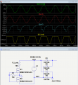
No, but the MOSFET bias will be incorrect.
Notice that the bridge rectifiers clamp the negative AC voltage to ground, which fouls up the MOSFET bias.
As shown below this means the M2 will conduct through its body diode for the negative half of the sinewave even when the gate voltage is zero.

upload_2017-1-10_13-48-29.png
 
Top