Load cell offset drift cancellation circuit

Thread Starter

cmartinez

Joined Jan 17, 2007
8,257
I've been working with load cells for a long time now, and one of the problems that I have not yet been able to solve to my satisfaction is offset drift. Offset drift is the drift in output voltage over time even when the cell is under no load.
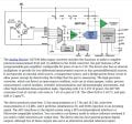
A while back, I found this very interesting circuit that excites the cell using a 400Hz AC signal:


Capture.JPG


Strain Gage Measurement Using An AC Excitation
Strain gage measurements are often plagued by offset drift, 1/f noise, and line noise. One solution is to use an ac signal to excite the bridge, as shown in Figure 6-14. The AD8221 gains the signal and an AD630AR synchronously demodulates the waveform. What results is a dc output proportional to the strain on the bridge. The output signal is devoid of all dc errors associated with the in-amp and the detector, including offset and offset drift.
In Figure 6-14, a 400 Hz signal excites the bridge. The signal at the AD8221’s input is an ac voltage. Similarly, the signal at the input of the AD630 is ac; the signal is dc at the end of the low-pass filter following the AD630.
The 400 Hz ac signal is rectified and then averaged; dc errors are converted in an ac signal and removed by the AD630. Ultimately, a precision dc signal is obtained.
The AD8221 is well-suited for this application because its high CMRR over frequency ensures that the signal of interest, which appears as a small difference voltage riding on a large sinusoidal common-mode voltage, is gained and the common-mode signal is rejected. In typical instrumentation amplifiers, CMRR falls off at about 200 Hz. In contrast, the AD8221 continues to reject common-mode signals beyond 10 kHz.
If an ac source is not available, a commutating voltage may be constructed using switches. The AD8221’s high CMRR over frequency rejects high frequency harmonics from a commutating voltage source.


I have several questions regarding this circuit:
  • Would the AC signal have to be precise and with zero-drift too? (I'm assuming that's a no)
  • Is there any other demodulator chip that could be used? The AD630 costs more than 20 bucks!
  • How precise would the ±15V sources have to be? Would simple 7815 and 7915 regulators do?
  • Is there a different circuit you may suggest that I should try, so as to accomplish my zero-drift goal?
Thanks everyone for your input
 

Thread Starter

cmartinez

Joined Jan 17, 2007
8,257
What are the load cells you have been using that is giving you the problem?
Max.
Trust me, I've been using quality load cells, such as Futek. And I'm still stuck with the same problem.
What I've done in the past to minimize it is excite the cell with the same reference source as the amplifier and the ADC, this way if the reference drifts over time, the rest of the circuit follows and almost cancels it.
How do commercial weight scales accomplish this? I've seen them in the market and they never drift, even when they've been turned on all day long!... though most of the time their resolution sucks too.
 

JohnInTX

Joined Jun 26, 2012
4,787
How do commercial weight scales accomplish this?
I did a couple that monitored the output with nothing on the scale. As the output drifted little bits over time, it adjusted the zero in firmware - kind of an auto tare. When weight was applied (bigger signal change) the latest 'zero' value was taken as the tare value. I was told that this was from a now-expired Ohaus patent - I just coded it. Worked perfectly - of course, you need the microcontroller. The excitation was DC referred to Vref.

Zero creep is one of many issues to think about. A considerable amount of our firmware was dedicated to load cell imperfections. Karl Hoffman's book is an excellent resource if you can find one.

Good luck.
 

Thread Starter

cmartinez

Joined Jan 17, 2007
8,257
I did a couple that monitored the output with nothing on the scale. As the output drifted little bits over time, it adjusted the zero in firmware - kind of an auto tare. When weight was applied (bigger signal change) the latest 'zero' value was taken as the tare value. I was told that this was from a now-expired Ohaus patent - I just coded it. Worked perfectly - of course, you need the microcontroller. The excitation was DC referred to Vref.

Zero creep is one of many issues to think about. A considerable amount of our firmware was dedicated to load cell imperfections. Karl Hoffman's book is an excellent resource if you can find one.

Good luck.
Thanks, I can use a microcontroller too, thank you very much. :cool:
Anyway, I'm looking into some other techniques as well, such as kelvin compensation.
 

OBW0549

Joined Mar 2, 2015
3,566
What I've done in the past to minimize it is excite the cell with the same reference source as the amplifier and the ADC, this way if the reference drifts over time, the rest of the circuit follows and almost cancels it.
In my opinion, that's as good as it gets with DC excitation: use a decent-quality reference voltage to excite the bridge, and use that same reference for the ADC which digitizes the bridge output. That will eliminate any excitation errors. You will still have temperature-induced shifts caused by input offset voltage tempco in the instrumentation amplifier, as well as thermocouple effects in the bridge itself and along the connection path to the amplifier; and the AC excitation design you cited will eliminate those errors.

But AC excitation will do nothing to help with shifts caused by temperature/aging that actually effects the load cell bridge balance, such as nonuniform thermal expansion or creep or improper mounting of the strain gage(s) in the load cell; those errors will still exist with the AC circuit, undiminished.

How do commercial weight scales accomplish this?
I think JohnInTX nailed it: strain gages and load cells are pesky little devices, and I don't know of any other solution but to implement some kind of tare function.
 

Thread Starter

cmartinez

Joined Jan 17, 2007
8,257
Ok, including a tare function in an MCU is easy enough... that means that the tare will be effected every few seconds or so, assuming that no load is placed on the load cell. So a minimum amount of load must be placed on the cell before a valid reading is taken then?
 

Thread Starter

cmartinez

Joined Jan 17, 2007
8,257
Sure, that will work, but only to eliminate the effects of offsets and offset tempco within the electronics. It doesn't help you any for errors originating within the gage.
Errors within the gage? other than temp drift? Would you mind elaborating?
 

OBW0549

Joined Mar 2, 2015
3,566
Errors within the gage? other than temp drift? Would you mind elaborating?
The stuff I mentioned in post #6 above: thermocouple effects in the bridge and along its connection path to the instrumentation, as well as shifts caused by temperature/aging that actually effect the load cell bridge balance, such as nonuniform thermal expansion or creep or improper mounting of the strain gage(s) in the load cell.
 

JohnInTX

Joined Jun 26, 2012
4,787
Re post #8, Microchip used a similar approach in their weight/loadcell demo kit a few years ago (sorry don't remember what it was called) to zap the offsets but OBW and I are in agreement.. You don't need any of that if you just monitor and adjust for ALL of the offsets and drift and lock in the current value when weight is applied. Most weight reading is done in a short time. This approach would fall apart in a non-scale application when weight/force will be applied for a long time. Then you would have to consider other factors.

Of course, during your short weigh-it-now approach, you still have to make sure your basic analog is up to snuff (sounds like it is).

Errors within the gage? other than temp drift? Would you mind elaborating?
Well, residual stresses, hysteresis, creep and the celebrated inhomogeneous strain field (which I just picked up scanning the index of the book previously referenced). The point is, a load cell combines some resistive circuit bonded to some metal which bends and transfers its stresses to the resistive part. There are lots of moving parts to all of it. Once past first-order analysis it becomes - fun.

I actually did read and (sort of ) understood the material in the book but found that, while understanding all of that is useful, in practice bringing firmware to bear on it pretty much swamps out most of those effects. You want a zero (described above) and a slope which we haven't discussed but - firmware again. YMMV

And for the record, I didn't do anything with the inhomogeneous strain field other than read about it. But its good to understand that for a good scale, you probably have to go past first-order thinking..

EDIT: and while typing, OBW provided similar illumination.. You really should buy that book. Its hard to find.

Keep in mind that Analog Devices sells analog solutions (and are stunningly good at doing so) but lots of that stuff can be done with a cheap uC and some *ahem* good firmware. The analog stuff includes quiet, short-term stable, ratiometric stuff into a good ADC. Then let the firmware take over.
 
Last edited:

Thread Starter

cmartinez

Joined Jan 17, 2007
8,257
Thank you John and OBW for your inputs, they're thoroughly appreciated. And OBW, sorry I made you repeat yourself, it's just that I thought that there was more than the things that had already been said.
And yes, I'm very much aware of cell creep, hysteresis, residual stresses and the like... which are all located in the cell itself and there's not much I can do about, except to tare or not to tare...

My main concern has been offset drift in the circuit itself, and on a minor scale in the cell. So maybe if I use the circuit I showed in post #8, with the analog switch placed real close to the ADC I might be able to cancel that, and also temperature changes in the cell, thermocoupling at the connection points in the cell, cable and PCB, and difference in resistivity due to cable lengths?
 

Thread Starter

cmartinez

Joined Jan 17, 2007
8,257
What level of performance have you achieved?
I've achieved 22 bit readings with only 2 bits of noise using a HI7190, which I now regret having selected for my project in the first place since it's a very expensive chip for what it does, and Analog Devices has chips of equal, or superior performance for 1/3 of the price.
I have not been able to get rid of the offset drift, even when I short the chip's inputs and no load cell is connected.
What level of performance do you desire?
I'd just like to have full 16-bit (or a little better) resolution at a high speed (at least 100 good solid readings per second) with a minimum of offset drift.
 

OBW0549

Joined Mar 2, 2015
3,566
I have not been able to get rid of the offset drift, even when I short the chip's inputs and no load cell is connected.
You're getting drift without the load cell connected, and with the ADC's inputs (or the inputs of whatever amplifier is feeding the ADC) shorted? How much drift, in terms of uV/C?
 

joeyd999

Joined Jun 6, 2011
5,285
I've achieved 22 bit readings with only 2 bits of noise using a HI7190, which I now regret having selected for my project in the first place since it's a very expensive chip for what it does, and Analog Devices has chips of equal, or superior performance for 1/3 of the price.
I have not been able to get rid of the offset drift, even when I short the chip's inputs and no load cell is connected.

I'd just like to have full 16-bit (or a little better) resolution at a high speed (at least 100 good solid readings per second) with a minimum of offset drift.
You haven't answered the question. Think in terms of analog -- we'll deal with digital later:

What is the capacity of the load cell?
What is the full scale output voltage (in mV/V)?
What is the zero offset (in mV/V)?
What is the tempco of zero and span?
What is the desired weight resolution (in commercial scales, this is called 'd' or number of divisions)?
 

Thread Starter

cmartinez

Joined Jan 17, 2007
8,257
You're getting drift without the load cell connected, and with the ADC's inputs (or the inputs of whatever amplifier is feeding the ADC) shorted? How much drift, in terms of uV/C?
You haven't answered the question. Think in terms of analog -- we'll deal with digital later:

What is the capacity of the load cell?
What is the full scale output voltage (in mV/V)?
What is the zero offset (in mV/V)?
What is the tempco of zero and span?
What is the desired weight resolution (in commercial scales, this is called 'd' or number of divisions)?
Those are all very good questions. Give me a day or two, and I'll come back with detailed answers.
In the meantime, thanks for trying to help me out here.
 

Thread Starter

cmartinez

Joined Jan 17, 2007
8,257
You haven't answered the question. Think in terms of analog -- we'll deal with digital later:
Load cell capacity: 200 lbs
All other info can be found in this figure:

Capture.JPG

At this point I'm more concerned about how to get maximum performance out a 24 bit ADC, and although I've been able to minimize noise, I have not yet been able to get the 16,777,216 (or ±8,388,608) divisions that its full scale is supposed to be able to deliver.
The cell is being excited with a 10VDC signal, which is delivered from a reference source, and its current then boosted through a transistor.
The ADC chip I'm using has an internal amplifier capable of gain of up to 128.

You're getting drift without the load cell connected, and with the ADC's inputs (or the inputs of whatever amplifier is feeding the ADC) shorted? How much drift, in terms of uV/C?
I have not actually measured that yet, but it's significant.

Would it help if I drew and posted a diagram of how the circuit that I'm using, and of the circuit I'm later planning to use?
 

Thread Starter

cmartinez

Joined Jan 17, 2007
8,257
For instance, how realistic is this circuit and what it claims?

Capture.JPG

Will it minimize drift? (I see that the load cell is being excited with 5V, and that it's not connected to ground, but rather to the chip's internal analog logic)

Here's the chip's datasheet.
 
Top