Calculating correct resistances for transistor circuit

Thread Starter

abelcorver

Joined Apr 10, 2010
14
Hey everyone,
I've been trying to understand (NPN) transistors (i.e. BJTs) for the past two weeks now. I think I understand the basic rules about active, saturation and cut-off now, and I even got some simple inverters to work.

However, they're probably drawing way too much current, and thus influencing the rest of my circuit. I chose my resistor value for the base transistor to be 100 ohms, however, that was like a complete guess, and it just worked, although only when operating alone... so not quite useful ...

So, I started reading a lot of texts about how to calculate the correct values.
My calculations can be found below...

So I want a couple of things to happen:
- The output of the inverter should be 20 mA and 2V
- Exactly all output current should be drawn by the collector of the transistor when I supply a 2V voltage on the base

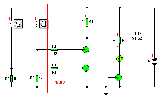
I calculated that R1 (see picture below) should be 50 ohms, and that was (probably :p) correct, since it seemed to work in a simulator. However, R2 probably isn't, and R3 is absurd (negative!) :p

I greatly appreciate any help!!
Thanks a lot in advance!

Regards,
Abel.

Original Size image


Jony130

Joined Feb 17, 2009
5,488
If you want saturation, then you must remove R2 and make Ib=Ic/10.

Or R2 = 0.5V/20mA = 25
and then Ib >> Ic/hfe_min = 2mA
R3 = (2V - 1.1V)/2mA = 450.

Or R3 = 0
And then R2 = (2V - 0.7V) / 40mA = 33

But in real life we never design BJt circuit like this.

Your assumptions are quite strange, normal if we wont IL=20mA we connect RL instead of Rc.
 
Last edited:

Thread Starter

abelcorver

Joined Apr 10, 2010
14
Ok, thanks a lot both of you. I think I'm starting to understand things a bit more... However, after reviewing what you guys said, I still can't get the following circuit to work (2 NAND flip-flop):


The current through the LEDs is 3,75 mA when ALL gates are open (sorry, the image has one gate closed, but the current through the LED is 3,75 mA when this one is open also). I have no idea how this is possible. I would expect 10 mA, since I calculated the following: U = 3V, I = 0,02A, so R = U / I = 150 ohms. Yeah, I forgot that the current would be split (that's true, right?), so wouldn't the current be 10 mA then?

I don't understand the other values either, so could anyone please explain to me how to tackle the circuit analysis of this circuit ?

Thanks a bunch in advance!

Regards,
Abel.
 

Thread Starter

abelcorver

Joined Apr 10, 2010
14
ok, sure.
This circuit (if I'm right at least), is a bistable flip-flop, and I want to use it as a memory cell. However, the problem is more general in my case:

I can't find a way to get multiple combinational gates (NAND gates in this case) to work together. For some reason, each time I connect the output of inverter A to the input of inverter B, both turn off. This is most probably due to wrong resistance values. So my question is: How can I calculate the correct values to use when I want to use them in such a situation.

Also, I don't understand why the simulator came up with such a strange current: 3,75 mA, while I would expect something like 10 mA. Once I understand why that is, I might also be able to answer the previous question, so answering either one works for me :)

Thanks in advance!

Regards,
Abel.
 

Jony130

Joined Feb 17, 2009
5,488
You circuit don't work propriety because you design it not quite right.
Look at proper design BJT "NAND" gate:


And simple RS flip-flop using only two BJT


And RS - flip-flop with BJT "NAND" gate


And in your circuit when all BJT are cut-off then you have two LED connect in parallel with 150 resistors in series connect to 3V power supply.
So from II KVL we have
Vcc= I*150Ω + VF
then if we assume VF = 1.6V then:
I = (3V - 1.6V) /150Ω = 9.3mA
So led current wll be lower then I_led = 9.3/2 (two diode in paraller) < 4.6mA, we don't know exact value, because we don't know the exact value for a diode voltage forward drop VF.
 

Thread Starter

abelcorver

Joined Apr 10, 2010
14
Thank you so much, this is all really helpful!!
I still have a few questions though (sorry, ;P)

(1) What does VF mean? Is it the collector-emitter voltages
of the two transistors in series added together?

(2) So did you use a 3rd transistor in order to draw higher
current through the LED ? Does this also prevent other things
from interferring with the LEDs current and voltage?

(3) How did you come up with the resistance values? The base resistor
value is chosen to draw one-tenth of the collector current, right?

(4) I wasn't able to create the second circuit in Yenka. What program
did you use?

(5) In the last circuit, when I change the 1K resistor values to lets say
100K, the current through the LED doesn't change (nicely done! :D).
Why is that? :)

(6) How did you learn all this :p haha again, thanks a lot (in advance)!

Regards,
Abel.
 
Last edited:

Jony130

Joined Feb 17, 2009
5,488
What does VF mean? Is it the collector-emitter voltages
of the two transistors in series added together?
VF is a LED forward voltage drop.
Collector-emitter voltages it would be Vce.
So did you use a 3rd transistor in order to draw higher
current through the LED ? Does this also prevent other things
from interferring with the LEDs current and voltage?
Well, yes.
This extra BJT acts like a "buffer" which separates LED from NAND gate.
Thanks to that extra BJT the LED does not effect the proper operation of the NAND gate.
How did you come up with the resistance values? The base resistor
value is chosen to draw one-tenth of the collector current, right?
Yes you right.
I always use Rb = Rc/( 0.1....0.5*Hfe_min) = Rc/ (10...50) to ensure saturation.
I wasn't able to create the second circuit in Yenka. What program
did you use?
Open the attached file in Yenka.
And the program I use is a older brother of a Yenka the crocodile clips.
http://www.mikrokontrolery.net/pawel/crocodile clips.rar

In the last circuit, when I change the 1K resistor values to lets say
100K, the current through the LED doesn't change (nicely done! :D).
Why is that?
That thanks to 3rd BJT and his current gain Hfe.
For example if BJT has Hfe=100 then for R =1K:
Base current is equal
Ib = (Vcc - Vbe) / (1K + 10K ) = ( 9V - 0.65V )/ 11KΩ = 760uA
And collector current
Ic = 100 * 760uA = 76mA
But in oner circuit is impassible to have Ic = 76mA because the max Ic is equal:
Ic_max = (Vcc - VF)/Rc = (9 - 2V)/470Ω = 14.9mA
So this means that BJT is in saturation.
And in saturation Ic = hfe * Ib don't hold anymore.
So in this circuit
Ib = 760uA
Ic = 14mA
Ie = Ib + Ic
And now if we change 1K resistor to 100K we get:
Ib = 8.35V / 110k =76uA
and Ic = 76uA * 100 = 7.6mA
And this time BJT is not in saturation because Ic < Ic_max.
So Vce = Vcc - VF - Ic*Rc = 9V - 2V - 7.6mA *470Ω = 3.4V

http://forum.allaboutcircuits.com/showthread.php?t=24314&highlight=saturation
http://forum.allaboutcircuits.com/showthread.php?p=166105#post166105
How did you learn all this
Well I read a lot, building a lot of simple and them more complicated circuit in breadboard and destroyed a few components.
I also have a lot of patience because electronics isn't easy.
 

Attachments

Thread Starter

abelcorver

Joined Apr 10, 2010
14
Thanks you SO much for all your amazing help!
This forum really is a great place, but more importantly, with great people.

Regards,
Abel.
 
Top